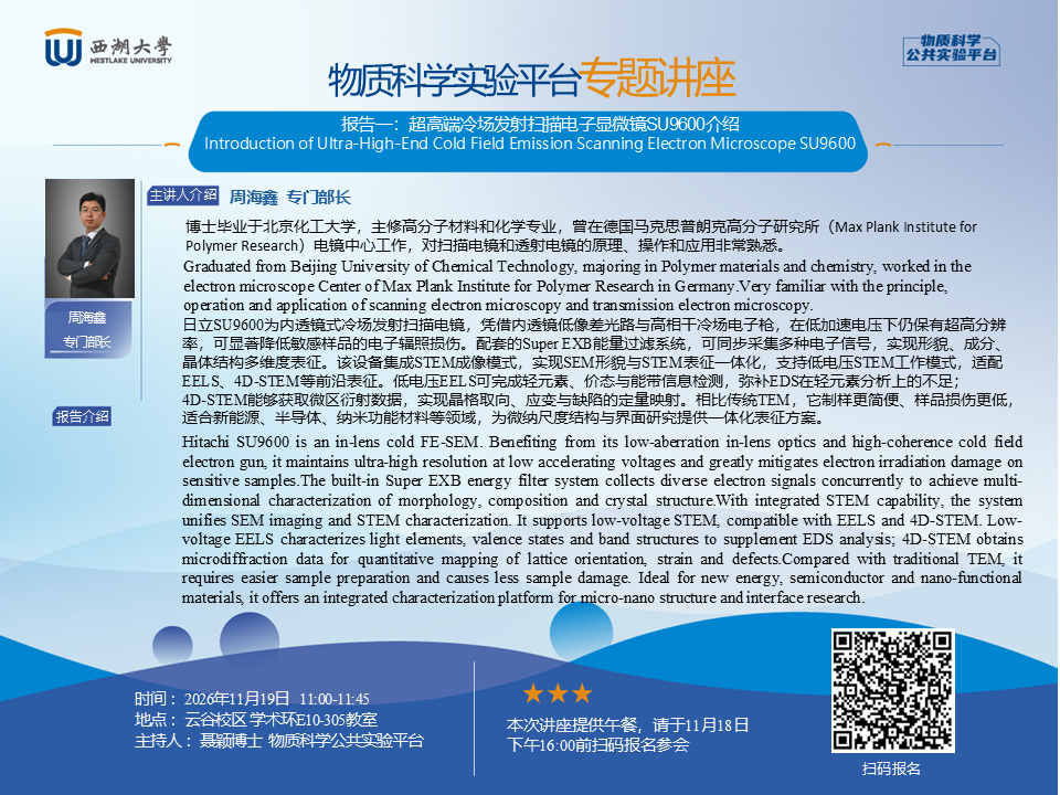
【 主 题 】:报告一、超高端冷场发射扫描电子显微镜SU9600介绍
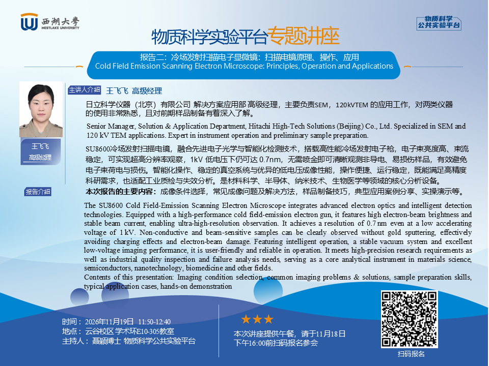
报告二、冷场发射扫描电子显微镜:扫描电镜原理、操作、应用
【 时 间 】:2026年11月19日(周四),11:00—13:00
【 地 点 】:云谷校区 E10-305教室
【主讲人】:周海鑫 专门部长/王飞飞 高级应用经理
【主持人】:聂颖 博士
【讲座语言】:中文
【 简 介 】:
报告一:日立SU9600为内透镜式冷场发射扫描电镜,凭借内透镜低像差光路与高相干冷场电子枪,在低加速电压下仍保有超高分辨率,可显著降低敏感样品的电子辐照损伤。配套的Super EXB能量过滤系统,可同步采集多种电子信号,实现形貌、成分、晶体结构多维度表征。该设备集成STEM成像模式,实现SEM形貌与STEM表征一体化,支持低电压STEM工作模式,适配EELS、4D‑STEM等前沿表征。低电压EELS可完成轻元素、价态与能带信息检测,弥补EDS在轻元素分析上的不足;4D‑STEM能够获取微区衍射数据,实现晶格取向、应变与缺陷的定量映射。相比传统TEM,它制样更简便、样品损伤更低,适合新能源、半导体、纳米功能材料等领域,为微纳尺度结构与界面研究提供一体化表征方案。
报告二:SU8600冷场发射扫描电镜,融合先进电子光学与智能化检测技术,搭载高性能冷场发射电子枪,电子束亮度高、束流稳定,可实现超高分辨率观察,1kV 低电压下仍可达 0.7nm,无需喷金即可清晰观测非导电、易损伤样品,有效避免电子束荷电与损伤。智能化操作、稳定的真空系统与优异的低电压成像性能,操作便捷、运行稳定,既能满足高精度科研需求,也适配工业质检与失效分析。是材料科学、半导体、纳米技术、生物医学等领域的核心分析设备。
本次报告的主要内容:成像条件选择,常见成像问题及解决方法,样品制备技巧,典型应用案例分享、实操演示等。
【报名方式】:讲座提供午餐,请于11月18日16:00前扫描下方二维码报名。
Dear Teachers and Students,
The Instrumentation and Service Center for Physical Sciences (ISCPS) will host a lunch seminar with two presentations titled “Introduction of Ultra-High-End Cold Field Emission Scanning Electron Microscope SU9600" and “Cold Field Emission Scanning Electron Microscope: Principles, Operation and Applications" on Thursday, November 19, 2026. Teachers and students who are interested are warmly welcome to register and attend.
Presentation One: Introduction of Ultra-High-End Cold Field Emission Scanning Electron Microscope SU9600
Presentation Two: Cold Field Emission Scanning Electron Microscope: Principles, Operation and Applications
Date & Time: Thursday, November 19, 2026, 11:00- 13:00
Venue: Classroom E10-305, Yungu Campus
Speaker: Haixin Zhou and Feifei Wang, Service Engineer
Host: Dr. Ying Nie
Language: Chinese
Introduction:
Presentation One: Hitachi SU9600 is an in-lens cold FE-SEM. Benefiting from its low-aberration in-lens optics and high-coherence cold field electron gun, it maintains ultra-high resolution at low accelerating voltages and greatly mitigates electron irradiation damage on sensitive samples.The built-in Super EXB energy filter system collects diverse electron signals concurrently to achieve multi-dimensional characterization of morphology, composition and crystal structure.With integrated STEM capability, the system unifies SEM imaging and STEM characterization. It supports low-voltage STEM, compatible with EELS and 4D‑STEM. Low-voltage EELS characterizes light elements, valence states and band structures to supplement EDS analysis; 4D‑STEM obtains microdiffraction data for quantitative mapping of lattice orientation, strain and defects.Compared with traditional TEM, it requires easier sample preparation and causes less sample damage. Ideal for new energy, semiconductor and nano-functional materials, it offers an integrated characterization platform for micro-nano structure and interface research.
Presentation Two: The SU8600 Cold Field‑Emission Scanning Electron Microscope integrates advanced electron optics and intelligent detection technologies. Equipped with a high‑performance cold field‑emission electron gun, it features high electron‑beam brightness and stable beam current, enabling ultra‑high‑resolution observation. It achieves a resolution of 0.7 nm even at a low accelerating voltage of 1 kV. Non‑conductive and beam‑sensitive samples can be clearly observed without gold sputtering, effectively avoiding charging effects and electron‑beam damage. Featuring intelligent operation, a stable vacuum system and excellent low‑voltage imaging performance, it is user‑friendly and reliable in operation. It meets high‑precision research requirements as well as industrial quality inspection and failure analysis needs, serving as a core analytical instrument in materials science, semiconductors, nanotechnology, biomedicine and other fields.
Contents of this presentation: Imaging condition selection, common imaging problems & solutions, sample preparation skills, typical application cases, hands-on demonstration.
Registration: Lunch provided. Please scan the QR code below to register.